VC Power SoM Hardware Operating Manual
Hardware specifications of VC Power SoMs and VC Power SoM Carrier Boards
| Revision: | 0.1 |
|---|---|
| Date: | 2023-11-16 |
| Contact: | support@vision-comp.com |
| Copyright: | 2023 Vision Components GmbH Ettlingen, Germany |
| Author: | VC Support, mailto:support@vision-comp.com |


This documentation has been prepared with most possible care. However Vision Components GmbH does not take any liability for possible errors. In the interest of progress, Vision Components GmbH reserves the right to perform technical changes without further notice.
Please notify support@vision-components.com if you become aware of any errors in this manual or if a certain topic requires more detailed documentation.
This manual is intended for information of Vision Component’s customers only. Any publication of this document or parts thereof requires written permission by Vision Components GmbH.
| Symbol | Meaning |
|---|---|
 |
The Light bulb highlights hints and ideas that may be helpful for a development. |
 |
This warning sign alerts of possible pitfalls to avoid. Please pay careful attention to sections marked with this sign. |
 |
This is a sign for an example. |
Trademarks
Linux, Debian, the Tux logo, Vivado, Xilinx and Zynq, ARM, Cortex, Windows XP, Total Commander, Tera Term, Motorola, HALCON, FreeRTOS, Vision Components are registered Trademarks. All trademarks are the property of their respective owners.
Nvidia, Jetson, Asus, Raspberry Pi and Raspbian are also registered Trademarks.
ESD sensitivity
Warning
The components are very sensitive to electrostatic
discharge (ESD)! Please take all the precautions necessary to avoid ESD!
ESD
 The electronic components and circuits are sensitive to ElectroStatic
Discharge (ESD). When handling any circuit board assemblies, it is
necessary that ESD safety precautions be observed.
The electronic components and circuits are sensitive to ElectroStatic
Discharge (ESD). When handling any circuit board assemblies, it is
necessary that ESD safety precautions be observed.
ESD safe best practices include, but are not limited to:
- Leaving circuit boards in their antistatic packaging until they are ready to be installed.
- Using a grounded wrist strap when handling circuit boards.
- Working on a grounded ESD table mat.
- Only handling circuit boards in ESD safe areas, which may include ESD floor and table mats, wrist strap stations and ESD safe lab coats.
- Avoiding handling circuit boards in carpeted areas.
- Try to handle the board by the edges, avoiding contact with components.
This note is not an exhaustive information about the protection against electrostatic discharge (ESD).
Table of Contents
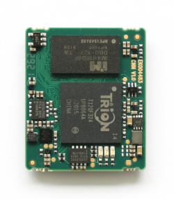
1 VC Power SoM
1.1 Features
- Efinix Trion T120 FPGA with 112128 Logic Elements
- 512MByte of DRAM onboard
- Boot QSPI flash and Data QSPI flash
- Operated with a single power supply 5V±5%
- FPGA and DRAM voltages (3.3V,1.5V,1.2V) are provided by the module
- Module performs power sequencing
- Carrier Board available
1.2 Block Diagram
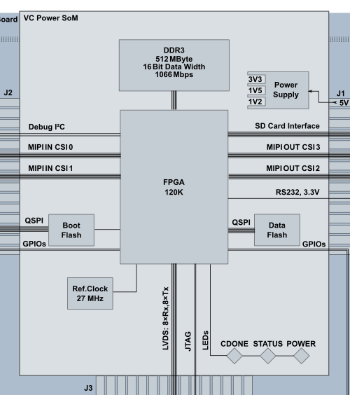
VC Power SoM Block Diagram
1.3 Technical Specification
| Component / Feature | Specification |
|---|---|
| FPGA | Efinix Trion T120F324C4 |
| Logic Elements | 112128 |
| Embedded RAM Bits (kb) | 5407 |
| Embedded 5K RAM Blocks | 1056 |
| 18x18 Multipliers | 320 |
| PLLs | 8 |
| Clock Signals | 16 |
| DDR3 (up to 1066 Mbps) | x16 (built-in DDR3 RAM controller) |
| Mipi 4-lane CSI-2 controller | 2 x RX plus 2 x TX |
| Number of lanes | 1–4 depending on sensor module |
| MIPI speed | max. 1.5Gbps |
| Boot Flash | 32MBit QSPI, Type: IS25LP032D (U7) |
| Data Flash | 32MBit QSPI, Type: IS25LP032D (U11) |
| Recommended Power Source | 5V, 1.5A |
| Power Consumption | max. 6W @ 5V depending on FPGA design |
| Reference Clock | 27MHz for FPGA PLLs: FPGA, DDR3 RAM, MIPI |
| Flash output signal | 3.3V LVCMOS |
| Trigger input signal | 3.3V LVCMOS |
| Dimensions | 28.5mm × 24mm |
| Storage Conditions | Temperature: -20 to +60 deg C, Max. humidity: 90%, non condensing. |
| Operating Conditions | Temperature: 0 to +50 deg C, Max. humidity: 80%, non condensing. |
1.4 LEDs
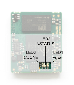
VC Power SoM LED Positions
| Function | Position | Bedeutung |
|---|---|---|
| power | LED1 | indicator for power supply |
| NSTATUS | LED2 | error indicator during programming,general purpose after programming |
| CDONE | LED3 | LED on only during programming |
1.5 Connectors
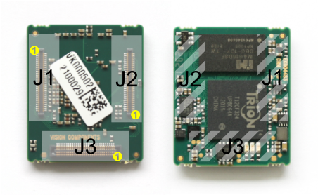
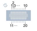
VC Power SoM Connector IDs
| ID | Type |
|---|---|
| J1, J2 | Kyocera 14-5804-060-050-829+ (plug) |
| J3 (optional) | Kyocera 24-5804-060-030-829+ (receptacle) |
1.5.1 J1: Power, CSI1/2 IN, SD card, RS232
| Class | Signal | Pin No. | Pin No. | Signal | Class | |
|---|---|---|---|---|---|---|
| GND | 1 |  |
60 | GND | ||
| MIPI OUT CSI 2 | cam2_sda | 2 | 59 | cam3_sda | MIPI OUT CSI 3 | |
| MIPI OUT CSI 2 | cam2_scl | 3 | 58 | cam3_scl | MIPI OUT CSI 3 | |
| GND | 4 | 57 | GND | |||
| MIPI OUT CSI 2 | cam2_flash | 5 | 56 | cam3_flash | MIPI OUT CSI 3 | |
| MIPI OUT CSI 2 | cam2_trig | 6 | 55 | cam3_trig | MIPI OUT CSI 3 | |
| GND | 7 | 54 | GND | |||
| MIPI OUT CSI 3 | CSI3_DATA1_P | 8 | 53 | CSI3_DATA3_P | MIPI OUT CSI 3 | |
| MIPI OUT CSI 3 | CSI3_DATA1_N | 9 | 52 | CSI3_DATA3_N | MIPI OUT CSI 3 | |
| GND | 10 | 51 | GND | |||
| MIPI OUT CSI 3 | CSI3_DATA0_P | 11 | 50 | CSI3_DATA2_P | MIPI OUT CSI 3 | |
| MIPI OUT CSI 3 | CSI3_DATA0_N | 12 | 49 | CSI3_DATA2_N | MIPI OUT CSI 3 | |
| GND | 13 | 48 | GND | |||
| MIPI OUT CSI 2 | CSI2_CLK_P | 14 | 47 | CSI3_CLK_P | MIPI OUT CSI 3 | |
| MIPI OUT CSI 2 | CSI2_CLK_N | 15 | 46 | CSI3_CLK_N | MIPI OUT CSI 3 | |
| GND | 16 | 45 | GND | |||
| MIPI OUT CSI 2 | CSI2_DATA1_P | 17 | 44 | CSI2_DATA3_P | MIPI OUT CSI 2 | |
| MIPI OUT CSI 2 | CSI2_DATA1_N | 18 | 43 | CSI2_DATA3_N | MIPI OUT CSI 2 | |
| GND | 19 | 42 | GND | |||
| MIPI OUT CSI 2 | CSI2_DATA0_P | 20 | 41 | CSI2_DATA2_P | MIPI OUT CSI 2 | |
| MIPI OUT CSI 2 | CSI2_DATA0_N | 21 | 40 | CSI2_DATA2_N | MIPI OUT CSI 2 | |
| GND | 22 | 39 | GND | |||
| SD Card Iface | SD_CLK | 23 | 38 | trig_sen0 | TRIG | |
| GND | 24 | 37 | flash_sen0 | FLASH | ||
| SD Card Iface | SD_DAT1 | 25 | 36 | gpio0 | GPIO | |
| SD Card Iface | SD_DAT0 | 26 | 35 | RS232_TxD | RS232 3.3V | |
| SD Card Iface | SD_CMD | 27 | 34 | RS232_RxD | RS232 3.3V | |
| SD Card Iface | SD_DAT3 | 28 | 33 | Vcc3V3 output 50mA | Power Output | |
| SD Card Iface | SD_DAT2 | 29 | 32 | Vcc5V0 input | Power Input | |
| GND | 30 | 31 | Vcc5V0 input | Power Input |
1.5.2 J2: CSI OUT 1/2, QSPI Programming
| Class | Signal | Pin No. | Pin No. | Signal | Class | |
|---|---|---|---|---|---|---|
| GND | 1 | |
60 | GND | ||
| MIPI IN CSI 0 | cam0_sda | 2 | 59 | cam1_sda | CSI1 RX | |
| MIPI IN CSI 0 | cam0_scl | 3 | 58 | cam1_scl | CSI1 RX | |
| GND | 4 | 57 | GND | |||
| MIPI IN CSI 0 | cam0_flash | 5 | 56 | cam1_flash | CSI1 RX | |
| MIPI IN CSI 0 | cam0_trig | 6 | 55 | cam1_trig | CSI1 RX | |
| GND | 7 | 54 | GND | |||
| MIPI IN CSI 1 | CSI1_CLK_P | 8 | 53 | CSI1_DATA3_P | CSI1 RX | |
| MIPI IN CSI 1 | CSI1_CLK_N | 9 | 52 | CSI1_DATA3_N | CSI1 RX | |
| GND | 10 | 51 | GND | |||
| MIPI IN CSI 1 | CSI1_DATA1_P | 11 | 50 | CSI1_DATA2_P | CSI1 RX | |
| MIPI IN CSI 1 | CSI1_DATA1_N | 12 | 49 | CSI1_DATA2_N | CSI1 RX | |
| GND | 13 | 48 | GND | |||
| MIPI IN CSI 1 | CSI1_DATA0_P | 14 | 47 | CSI0_CLK_P | CSI1 RX | |
| MIPI IN CSI 1 | CSI1_DATA0_N | 15 | 46 | CSI0_CLK_N | CSI1 RX | |
| GND | 16 | 45 | GND | |||
| MIPI IN CSI 0 | CSI0_DATA1_P | 17 | 44 | CSI0_DATA2_P | CSI0 RX | |
| MIPI IN CSI 0 | CSI0_DATA1_N | 18 | 43 | CSI0_DATA2_N | CSI0 RX | |
| GND | 19 | 42 | GND | |||
| MIPI IN CSI 0 | CSI0_DATA0_P | 20 | 41 | CSI0_DATA3_P | CSI0 RX | |
| MIPI IN CSI 0 | CSI0_DATA0_N | 21 | 40 | CSI0_DATA3_N | CSI0 RX | |
| GND | 22 | 39 | GND | |||
| Debugging | dbg_sck | 23 | 38 | trig_sen1 | TRIG | |
| Debugging | dbg_sda | 24 | 37 | flash_sen1 | FLASH | |
| QSPI | QSPI_CCK | 25 | 36 | do not connect | ||
| QSPI | QSPI_CSn | 26 | 35 | do not connect | ||
| QSPI | QSPI_CDI0 | 27 | 34 | do not connect | ||
| QSPI | QSPI_CDI1 | 28 | 33 | do not connect | ||
| NC | 29 | 32 | NC | |||
| NC | 30 | 31 | NC |
1.5.3 J3 (optional): LVDS, JTAG
| Class | Signal | Pin No. | Pin No. | Signal | Class | |
|---|---|---|---|---|---|---|
| JTAG | T120_TMS | 60 |  |
1 | T120_TDO JTAG | JTAG |
| JTAG | T120_TCK | 59 | 2 | T120_TDI JTAG | JTAG | |
| GND | 58 | 3 | GND | |||
| LVDS | tx00_p | 57 | 4 | rx00_p LVDS | LVDS | |
| LVDS | tx00_n | 56 | 5 | rx00_n LVDS | LVDS | |
| GND | 55 | 6 | GND | |||
| LVDS | tx01_p | 54 | 7 | rx01_p LVDS | LVDS | |
| LVDS | tx01_n | 53 | 8 | rx01_n LVDS | LVDS | |
| GND | 52 | 9 | GND | |||
| LVDS | tx02_p | 51 | 10 | rx02_p LVDS | LVDS | |
| LVDS | tx02_n | 50 | 11 | rx02_n LVDS | LVDS | |
| GND | 49 | 12 | GND | |||
| LVDS | tx03_p | 48 | 13 | rx03_p LVDS | LVDS | |
| LVDS | tx03_n | 47 | 14 | rx03_n LVDS | LVDS | |
| GND | 46 | 15 | GND | |||
| LVDS | tx04_p | 45 | 16 | clk1_p LVDS | LVDS | |
| LVDS | tx04_n | 44 | 17 | clk1_n LVDS | LVDS | |
| GND | 43 | 18 | GND | |||
| LVDS | tx05_p | 42 | 19 | rx04_p LVDS | LVDS | |
| LVDS | tx05_n | 41 | 20 | rx04_n LVDS | LVDS | |
| GND | 40 | 21 | GND | |||
| LVDS | tx06_p | 39 | 22 | rx05_p LVDS | LVDS | |
| LVDS | tx06_n | 38 | 23 | rx05_n LVDS | LVDS | |
| GND | 37 | 24 | GND | |||
| LVDS | tx07_p | 36 | 25 | rx06_p LVDS | LVDS | |
| LVDS | tx07_n | 35 | 26 | rx06_n LVDS | LVDS | |
| GND | 34 | 27 | GND | |||
| LVDS | tx08_p | 33 | 28 | rx07_p LVDS | LVDS | |
| LVDS | tx08_n | 32 | 29 | rx07_n LVDS | LVDS | |
| GND | 31 | 30 | GND |
1.5.4 VC Power SoM FPGA Pin Signals
| Pin Names | Pin ID | Signal Name |
|---|---|---|
| CDONE | N18 | CDONE |
| CRESET_N | N17 | CRESET_N |
| GPIOL_04_CSI | N15 | CSI |
| TCK | T16 | TCK |
| TDI | R16 | TDI |
| TDO | P17 | TDO |
| TMS | P16 | TMS |
| GPIOL_18_CDI4 | M18 | conf_sck |
| GPIOL_20_CDI5 | L18 | conf_csn |
| GPIOL_22_CDI6 | L16 | conf_dat0 |
| GPIOL_24_CDI7 | L17 | conf_dat1 |
| GPIOL_15_PLLIN0 | L14 | conf_dat2 |
| GPIOL_17_EXTFB0 | L15 | conf_dat3 |
| GPIOL_62_CTRL0 | K16 | SD_DAT3 |
| GPIOL_63_CTRL1 | K15 | SD_CMD |
| GPIOL_66_CLK0 | K17 | SD_DAT2 |
| GPIOL_72_CLK6 | H14 | SD_DAT0 |
| GPIOL_73_CLK7 | H13 | SD_CLK |
| GPIOL_75_CTRL5 | G13 | SD_DAT1 |
| GPIOL_156_CBSEL0 | J17 | CBSEL0 |
| GPIOL_157_CBSEL1 | J18 | CBSEL1 |
| GPIOL_150_NSTATUS | J14 | NSTATUS |
| GPIOL_151_TEST_N | J15 | TEST_N |
| GPIOT_RXN01 | C13 | cam3_flash |
| GPIOT_RXN02 | D16 | cam2_trig |
| GPIOT_RXN03 | C11 | cam3_trig |
| GPIOT_RXN04 | E15 | cam2_flash |
| GPIOT_RXN05 | E14 | cam0_sda |
| GPIOT_RXN06 | D12 | cam1_sda |
| GPIOT_RXN07 | F13 | cam0_scl |
| GPIOT_RXN08_EXTFB0 | F11 | cam0_trig |
| GPIOT_RXP01 | D13 | cam3_scl |
| GPIOT_RXP02 | C16 | cam2_scl |
| GPIOT_RXP03 | D11 | cam1_scl |
| GPIOT_RXP04 | D15 | cam2_sda |
| GPIOT_RXP05 | D14 | cam3_sda |
| GPIOT_RXP06 | E12 | cam1_flash |
| GPIOT_RXP07 | E13 | cam0_flash |
| GPIOT_RXP08_EXTFB0 | E11 | cam1_trig |
| GPIOT_RXN11 | H17 | rx00_n |
| GPIOT_RXN12 | H16 | rx01_n |
| GPIOT_RXN13 | H15 | rx02_n |
| GPIOT_RXN14 | F14 | rx03_n |
| GPIOT_RXN15 | E17 | rx04_n |
| GPIOT_RXN16 | E18 | rx05_n |
| GPIOT_RXN17 | G18 | rx06_n |
| GPIOT_RXN18_EXTFB1 | C18 | rx07_n |
| GPIOT_RXN19_CLKN1 | B17 | clk1_n |
| GPIOT_RXP11 | G17 | rx00_p |
| GPIOT_RXP12 | G16 | rx01_p |
| GPIOT_RXP13 | G15 | rx02_p |
| GPIOT_RXP14 | G14 | rx03_p |
| GPIOT_RXP15 | D17 | rx04_p |
| GPIOT_RXP16 | D18 | rx05_p |
| GPIOT_RXP17 | H18 | rx06_p |
| GPIOT_RXP18_EXTFB1 | B18 | rx07_p |
| GPIOT_RXP19_CLKP1 | A17 | clk1_p |
| GPIOT_RXN28_EXTFB2 | B10 | trig_sen0 |
| GPIOT_RXN29_CLKN2 | A9 | RS232_TxD |
| GPIOT_RXP27 | A11 | flash_sen0 |
| GPIOT_RXP28_EXTFB2 | A10 | gpio0 |
| GPIOT_RXP29_CLKP2 | B9 | RS232_RxD |
| MIPI0_RXDN0 | D5 | CSI1_DATA0_N |
| MIPI0_RXDN1 | D8 | CSI1_CLK_N |
| MIPI0_RXDN2 | F5 | CSI1_DATA1_N |
| MIPI0_RXDN3 | D6 | CSI1_DATA2_N |
| MIPI0_RXDN4 | F7 | CSI1_DATA3_N |
| MIPI0_RXDP0 | E5 | CSI1_DATA0_P |
| MIPI0_RXDP1 | E8 | CSI1_CLK_P |
| MIPI0_RXDP2 | F6 | CSI1_DATA1_P |
| MIPI0_RXDP3 | E6 | CSI1_DATA2_P |
| MIPI0_RXDP4 | E7 | CSI1_DATA3_P |
| MIPI0_TXDN0 | A6 | CSI2_DATA1_N |
| MIPI0_TXDN1 | B7 | CSI2_DATA2_N |
| MIPI0_TXDN2 | A8 | CSI2_DATA0_N |
| MIPI0_TXDN3 | B5 | CSI2_DATA3_N |
| MIPI0_TXDN4 | B4 | CSI2_CLK_N |
| MIPI0_TXDP0 | B6 | CSI2_DATA1_P |
| MIPI0_TXDP1 | A7 | CSI2_DATA2_P |
| MIPI0_TXDP2 | B8 | CSI2_DATA0_P |
| MIPI0_TXDP3 | A5 | CSI2_DATA3_P |
| MIPI0_TXDP4 | A4 | CSI2_CLK_P |
| MIPI1_RXDN0 | E4 | CSI0_CLK_N |
| MIPI1_RXDN1 | G3 | CSI0_DATA1_N |
| MIPI1_RXDN2 | F1 | CSI0_DATA0_N |
| MIPI1_RXDN3 | G2 | CSI0_DATA2_N |
| MIPI1_RXDN4 | E3 | CSI0_DATA3_N |
| MIPI1_RXDP0 | D4 | CSI0_CLK_P |
| MIPI1_RXDP1 | F3 | CSI0_DATA1_P |
| MIPI1_RXDP2 | G1 | CSI0_DATA0_P |
| MIPI1_RXDP3 | H2 | CSI0_DATA2_P |
| MIPI1_RXDP4 | D3 | CSI0_DATA3_P |
| MIPI1_TXDN0 | A3 | CSI3_DATA0_N |
| MIPI1_TXDN1 | A2 | CSI3_DATA1_N |
| MIPI1_TXDN2 | B1 | CSI3_DATA2_N |
| MIPI1_TXDN3 | E2 | CSI3_CLK_N |
| MIPI1_TXDN4 | D1 | CSI3_DATA3_N |
| MIPI1_TXDP0 | B3 | CSI3_DATA0_P |
| MIPI1_TXDP1 | B2 | CSI3_DATA1_P |
| MIPI1_TXDP2 | C1 | CSI3_DATA2_P |
| MIPI1_TXDP3 | D2 | CSI3_CLK_P |
| MIPI1_TXDP4 | E1 | CSI3_DATA3_P |
| DDR_A[0] | P3 | DDR3.A0 |
| DDR_A[1] | P4 | DDR3.A1 |
| DDR_A[10] | V7 | DDR3.A10 |
| DDR_A[11] | U7 | DDR3.A11 |
| DDR_A[12] | U6 | DDR3.A12 |
| DDR_A[13] | T6 | DDR3.A13 |
| DDR_A[14] | V6 | DDR3.A14 |
| DDR_A[15] | V5 | DDR3.A15 |
| DDR_A[2] | R6 | DDR3.A2 |
| DDR_A[3] | P6 | DDR3.A3 |
| DDR_A[4] | T1 | DDR3.A4 |
| DDR_A[5] | R3 | DDR3.A5 |
| DDR_A[6] | R7 | DDR3.A6 |
| DDR_A[7] | V8 | DDR3.A7 |
| DDR_A[8] | T4 | DDR3.A8 |
| DDR_A[9] | T3 | DDR3.A9 |
| DDR_BA[0] | T5 | DDR3.BA0 |
| DDR_BA[1] | U3 | DDR3.BA1 |
| DDR_BA[2] | R5 | DDR3.BA2 |
| DDR_CAS_N | V2 | DDR3.nCAS |
| DDR_CK | P1 | DDR3.CLK_p |
| DDR_CK_N | R1 | DDR3.CLK_n |
| DDR_CKE | N7 | DDR3.CKE |
| DDR_CS_N | N6 | DDR3.nCS |
| DDR_DM[0] | L1 | DDR3.DM0 |
| DDR_DM[1] | H5 | DDR3.DM1 |
| DDR_DQ[0] | N4 | DDR3.D0 |
| DDR_DQ[1] | N2 | DDR3.D1 |
| DDR_DQ[10] | J3 | DDR3.D10 |
| DDR_DQ[11] | K3 | DDR3.D11 |
| DDR_DQ[12] | J4 | DDR3.D12 |
| DDR_DQ[13] | H4 | DDR3.D13 |
| DDR_DQ[14] | J5 | DDR3.D14 |
| DDR_DQ[15] | G4 | DDR3.D15 |
| DDR_DQ[2] | N1 | DDR3.D2 |
| DDR_DQ[3] | M2 | DDR3.D3 |
| DDR_DQ[4] | M4 | DDR3.D4 |
| DDR_DQ[5] | L3 | DDR3.D5 |
| DDR_DQ[6] | K1 | DDR3.D6 |
| DDR_DQ[7] | L4 | DDR3.D7 |
| DDR_DQ[8] | J1 | DDR3.D8 |
| DDR_DQ[9] | K2 | DDR3.D9 |
| DDR_DQS[0] | M3 | DDR3.DQS0_p |
| DDR_DQS[1] | K5 | DDR3.DQS1_p |
| DDR_DQS_N[0] | N3 | DDR3.DQS0_n |
| DDR_DQS_N[1] | L5 | DDR3.DQS1_n |
| DDR_ODT | U1 | DDR3.ODT |
| DDR_RAS_N | V3 | DDR3.nRAS |
| DDR_RST_N | T2 | DDR3.nReset |
| DDR_VREF | M6 | DDR3.CA_DQ_Vref |
| DDR_WE_N | U4 | DDR3.nWE |
| GPIOB_TXN17_CDI10 | U9 | flash_sen1 |
| GPIOB_TXP17_CDI11 | V9 | dbg_sda |
| GPIOB_TXN15_CDI14 | V10 | dbg_sck |
| GPIOB_TXP15_CDI15 | U10 | trig_sen1 |
| GPIOB_TXN08_CDI20 | U13 | tx08_n |
| GPIOB_TXP08_CDI21 | V13 | tx08_p |
| GPIOB_TXN07_CDI22 | R14 | tx07_n |
| GPIOB_TXP07_CDI23 | P14 | tx07_p |
| GPIOB_TXN06_CDI24 | U14 | tx06_n |
| GPIOB_TXP06_CDI25 | V14 | tx06_p |
| GPIOB_TXN05_CDI26 | R15 | tx05_n |
| GPIOB_TXP05_CDI27 | T15 | tx05_p |
| GPIOB_TXN04_CDI28 | V15 | tx04_n |
| GPIOB_TXP04_CDI29 | U15 | tx04_p |
| GPIOB_TXN03_CDI30 | V16 | tx03_n |
| GPIOB_TXP03_CDI31 | U16 | tx03_p |
| GPIOB_TXN00 | R17 | tx00_n |
| GPIOB_TXN01 | T18 | tx01_n |
| GPIOB_TXN02 | P18 | tx02_n |
| GPIOB_TXN09 | R13 | tx09_n |
| GPIOB_TXP00 | T17 | tx00_p |
| GPIOB_TXP01 | U18 | tx01_p |
| GPIOB_TXP02 | R18 | tx02_p |
| GPIOB_TXP09 | P13 | tx09_p |
| GPIOR_186_PLLIN0 | U8 | clk27mhz |
| GPIOR_187_PLLIN1 | T8 | clk27mhz |
| GPIOR_169_MREFCLK | F10 | clk27mhz |
1.6 Working Principle
On power-up the program is loaded into the FPGA with the built-in controller (SPI active x4 mode).
The reference clock is connected to mrefclk (Pin F10), pll_in0 (Pin U8) and pll_in1 (Pin T8)
2 VC Power SoM Carrier Board
2.1 Features
- Single Power Supply 12–24V, 12W
- Two 22-pin MIPI-In Connectors
- Two 22-pin MIPI-Out Connectors
- Micro-SD card slot
- Main Connector with LVTTL3V3 signals
- RS232 interface level shifter
2.2 Block Diagram

VC Power SoM Carrier Board with VC Power SoM Block Diagram
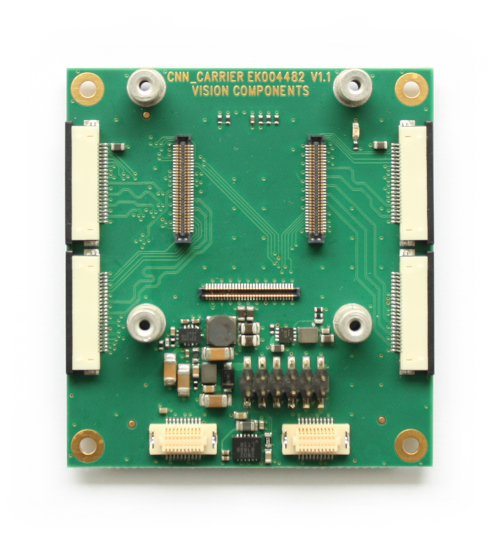
Carrier Board Front view

Carrier Board Back view
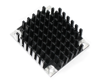
VC Power SoM Carrier Board Heat Sink
Based on the power consumption you are encouraged to cool the VC Power SoM, for example with the VC Power SoM Carrier Board Heat Sink.
2.3 LEDs

VC Power SoM Carrier Board LED Positions
| Function | Position | Bedeutung |
|---|---|---|
| power | LED1 | indicator for power supply |
2.4 Connectors
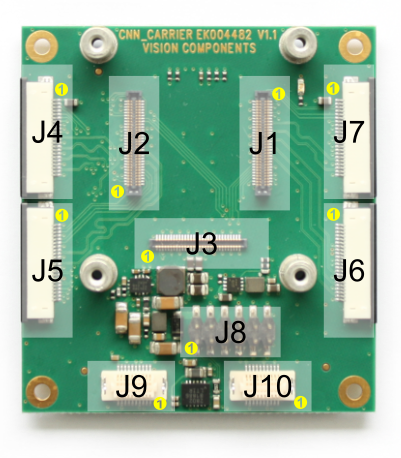
Carrier Board Connector IDs
| ID | Type |
|---|---|
| J1, J2 | Kyocera 24-5804-060-030-829+ (receptacle) |
| J3 (optional) | Kyocera 14-5804-060-050-829+ (plug) |
| J4, J5, J6, J7 | JST 22FLZ-RSM2-TB |
| J8 | 2 mm header 151118-1062 |
| J9, J10 | JST 20R-JMDSS-G-1-TF |
| J11 (MicroSD) | standard Micro-SD socket |
2.4.1 J1, J2, J3: See VC Power SoM
For a description of the connectors J1 to J3 see the description at the VC Power SoM (same numbering).
2.4.2 J4: MIPI OUT CSI 0
| Pin No. | Signal | |
|---|---|---|
 |
1 | Vcc3V3 |
| 2 | cam0_sda | |
| 3 | cam0_scl | |
| 4 | GND | |
| 5 | cam0_flash | |
| 6 | cam0_trig | |
| 7 | GND | |
| 8 | CSI0_DATA3_P | |
| 9 | CSI0_DATA3_N | |
| 10 | GND | |
| 11 | CSI0_DATA2_P | |
| 12 | CSI0_DATA2_N | |
| 13 | GND | |
| 14 | CSI0_CLK_P | |
| 15 | CSI0_CLK_N | |
| 16 | GND | |
| 17 | CSI0_DATA1_P | |
| 18 | CSI0_DATA1_N | |
| 19 | GND | |
| 20 | CSI0_DATA0_P | |
| 21 | CSI0_DATA0_N | |
| 22 | GND |
2.4.3 J5: MIPI OUT CSI 1
| Pin No. | Signal | |
|---|---|---|
|
1 | Vcc3V3 |
| 2 | cam1_sda | |
| 3 | cam1_scl | |
| 4 | GND | |
| 5 | cam1_flash | |
| 6 | cam1_trig | |
| 7 | GND | |
| 8 | CSI1_DATA3_P | |
| 9 | CSI1_DATA3_N | |
| 10 | GND | |
| 11 | CSI1_DATA2_P | |
| 12 | CSI1_DATA2_N | |
| 13 | GND | |
| 14 | CSI1_CLK_P | |
| 15 | CSI1_CLK_N | |
| 16 | GND | |
| 17 | CSI1_DATA1_P | |
| 18 | CSI1_DATA1_N | |
| 19 | GND | |
| 20 | CSI1_DATA0_P | |
| 21 | CSI1_DATA0_N | |
| 22 | GND |
2.4.4 J6: MIPI OUT CSI 2
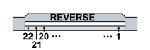
Note
Unusual Reverse Connector Numbering for J6 compared to J4/J5!
| Pin No. | Signal | |
|---|---|---|
 |
22 | GND |
| 21 | CSI2_DATA0_N | |
| 20 | CSI2_DATA0_P | |
| 19 | GND | |
| 18 | CSI2_DATA1_N | |
| 17 | CSI2_DATA1_P | |
| 16 | GND | |
| 15 | CSI2_CLK_N | |
| 14 | CSI2_CLK_P | |
| 13 | GND | |
| 12 | CSI2_DATA2_N | |
| 11 | CSI2_DATA2_P | |
| 10 | GND | |
| 9 | CSI2_DATA3_N | |
| 8 | CSI2_DATA3_P | |
| 7 | GND | |
| 6 | cam2_trig | |
| 5 | cam2_flash | |
| 4 | GND | |
| 3 | cam2_scl | |
| 2 | cam2_sda | |
| 1 | NC |
2.4.5 J7: MIPI OUT CSI 3
Note
Unusual Reverse Connector Numbering for J7 compared to J4/J5!
| Pin No. | Signal | |
|---|---|---|
|
22 | GND |
| 21 | CSI3_DATA0_N | |
| 20 | CSI3_DATA0_P | |
| 19 | GND | |
| 18 | CSI3_DATA1_N | |
| 17 | CSI3_DATA1_P | |
| 16 | GND | |
| 15 | CSI3_CLK_N | |
| 14 | CSI3_CLK_P | |
| 13 | GND | |
| 12 | CSI3_DATA2_N | |
| 11 | CSI3_DATA2_P | |
| 10 | GND | |
| 9 | CSI3_DATA3_N | |
| 8 | CSI3_DATA3_P | |
| 7 | GND | |
| 6 | cam3_trig | |
| 5 | cam3_flash | |
| 4 | GND | |
| 3 | cam3_scl | |
| 2 | cam3_sda | |
| 1 | NC |
2.4.6 J8: Main Connector
| Pin No. | Signal | |
|---|---|---|
 |
1 | SIG_TxD |
| 2 | C24V input | |
| 3 | SIG_RxD | |
| 4 | GND | |
| 5 | trig_sen0 (GPIO, 3.3V) | |
| 6 | trig_sen1 (GPIO, 3.3V) | |
| 7 | flash_sen0 (GPIO, 3.3V) | |
| 8 | flash_sen1 (GPIO, 3.3V) | |
| 9 | Vcc3V3 output | |
| 10 | gpio0 (GPIO, 3.3V) | |
| 11 | GND | |
| 12 | Vcc5V0 output |
2.4.7 J9: Programming Interface
| Pin No. | Signal | |
|---|---|---|
 |
1 | Vcc3V3 |
| 2 | GND | |
| 3 | QSPI_CCK | |
| 4 | GND | |
| 5 | QSPI_CSn | |
| 6 | QSPI_CDI1 | |
| 7 | GND | |
| 8 | QSPI_CDI0 | |
| 9 | NC | |
| 10 | GND | |
| 11 | NC | |
| 12 | NC | |
| 13 | do not connect | |
| 14 | NC | |
| 15 | do not connect | |
| 16 | do not connect | |
| 17 | GND | |
| 18 | do not connect | |
| 19 | GND | |
| 20 | Vcc3V3 |
2.4.8 J10: JTAG Connector
| Pin No. | Signal | |
|---|---|---|
|
1 | Vcc3V3 |
| 2 | GND | |
| 3 | NC | |
| 4 | GND | |
| 5 | NC | |
| 6 | dbg_sck (GPIO, 3.3V) | |
| 7 | GND | |
| 8 | dbg_sda (GPIO, 3.3V) | |
| 9 | NC | |
| 10 | GND | |
| 11 | NC | |
| 12 | NC | |
| 13 | T120_TDO (JTAG) | |
| 14 | NC | |
| 15 | T120_TDI (JTAG) | |
| 16 | T120_TMS (JTAG) | |
| 17 | GND | |
| 18 | T120_TCK (JTAG) | |
| 19 | GND | |
| 20 | Vcc3V3 |
3 Ordering Information
3.1 MIPI camera module order numbers
| Order Number | Product ID / Service description |
|---|---|
| VK000502 | VC Power SoM |
| VK000501 | VC Power SoM Carrier Board — do not forget to order the appropriate FPC cable! |
| VK?????? | VC Power SoM Carrier Board Heat Sink |
| Order Number | Product / Service description |
|---|---|
| EK003260 | Flexible Printed Circuit (FPC) Cable, 200 mm: 22 to 22 Pin |
| EK003261 | Flexible Printed Circuit (FPC) Cable, 200 mm: 22 to 15 Pin |
4 Appendix A: Dimensions VC Power SoM and VC Power SoM Carrier Board

Dimensions of the VC Power SoM
The .step file here provides exact positions of the VC Power SoM sockets.
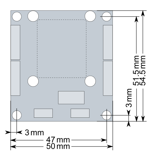
Dimensions of the VC Power SoM Carrier Board